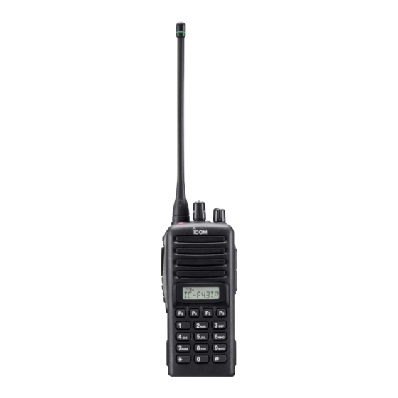
Icom IC-F43TR Service Manual
Uhf trunked radio
Hide thumbs
Also See for IC-F43TR:
- Instruction manual (32 pages) ,
- Instruction manual (40 pages) ,
- Instruction manual (40 pages)
Table of Contents
Advertisement
Quick Links
Download this manual
See also:
Instruction Manual
Advertisement
Table of Contents

Related Manuals for Icom IC-F43TR


Summary of Contents for Icom IC-F43TR
- Page 1 SERVICE MANUAL UHF TRUNKED RADIO F43TR...
- Page 2 8. READ the instructions of test equipment thoroughly before connecting equipment to the transceiver. Icom, Icom Inc. and are registered trademarks of Icom Incorporated (Japan) in the United States, the United Kingdom, Germany, France, Spain, Russia and/or other countries.
-
Page 3: Table Of Contents
TABLE OF CONTENTS SECTION SPECIFICATIONS SECTION INSIDE VIEWS SECTION DISASSEMBLY INSTRUCTIONS SECTION CIRCUIT DESCRIPITON RECEIVER CIRCUITS ........... . . 4-1 TRANSMITTER CIRCUITS . - Page 4 SECTION 1 SPECIFICATIONS ‘ ‘ GENERAL • Frequency coverage : 400.000–470.000 MHz [H] 450.000–512.000 MHz [L] • Mode : FM • Type of emission : 16K0F3E (25.0 kHz) WIDE 11K0F3E (12.5 kHz) NARROW • Number of conventional channels : 250 ch : 50 Ω...
-
Page 5: Section 2 Inside Views
SECTION 2 INSIDE VIEWS • MAIN UNIT TOP VIEW BOTTOM VIEW AF amplifier +5 Regulator APC amplifier (IC15: TA7568F) (IC17: NJM2870) (IC16: TA75S01F) IF amplifier Mute switch TX/RX switch (Q7: 2SC4215) (D29: MA2S111) (D16,D17: MA77) IF IC (IC9: TA31136FN) VCO circuit PLL IC R5 Regulator (IC21: LMX2352TM) -
Page 6: Section 3 Disassembly Instructions
SECTION 3 DISASSEMBLY INSTRUCTIONS • • REMOVING THE PA UNIT REMOVING THE CHASSIS UNIT 1 Unscrew 3 screws M. 1 Unscrew 1 nut A, and remove 2 knobs B,c. 2 Unscrew 2 screws D. 2 Unsolder 4 points N, and take off the PA unit in the direc- 3 Unscrew 2 screws E. -
Page 7: Receiver Circuits
SECTION 4 CIRCUIT DESCRIPTION 4-1 RECEIVER CIRCUITS The RF signals from the bandpass filter are mixed with the 4-1-1 ANTENNA SWITCHING CIRCUIT (PA UNIT) 1st LO signals, where come from the RX VCO circuit via the The antenna switching circuit functions as a low-pass filter low-pass filter (L46, C396, C397), at the 1st mixer circuit while receiving and a resonator circuit while transmitting. -
Page 8: Transmitter Circuits
4-1-5 AF AMPLIFIER CIRCUIT (MAIN UNIT) • CTCSS AND DTCS The tone squelch circuit detects AF signals and opens the The AF amplifier circuit amplifies the demodulated AF sig- squelch only when receiving a signal containing a matching nals to drive a speaker. This transceiver employs the base subaudible tone (CTCSS or DTCS). -
Page 9: Pll Circuits
4-2-2 MODULATION CIRCUIT (MAIN UNIT) 4-2-4 APC CIRCUIT (PA AND MAIN UNITS) The modulation circuit modulates the VCO oscillating signal The APC circuit protects the drive and power amplifiers from (RF signal) using the microphone audio signals. excessive current drive, and selects output power of HIGH or LOW. -
Page 10: Power Supply Circuits
4-4 POWER SUPPLY CIRCUIT The PLL IC contains a prescaler, programmable counter, programmable divider and phase detector, etc. The entered 4-4-1 MAIN UNIT VOLTAGE LINE signal is divided at the prescaler and programmable counter LINE DESCRIPTION section by the N-data ratio from the CPU. The divided signal is detected on phase at the phase detector using the refer- The voltage from the connected battery pack. -
Page 11: Other Circuits
4-6 PORT ALLOCATIONS 4-5 OTHER CIRCUITS 4-6-1 D/A CONVERTOR IC (IC12) 4-5-1 COMPOUNDER CIRCUIT (MAIN UNIT) IC-F43TR have compounder circuit which can improve S/N Port Description ratio and become wide dynamic range to suppress the number name transmitting signal and to extend receiving signal. The circuit Outputs the modulation balance level is composed of the base band IC (IC14). - Page 12 4-6-2 CPU (MAIN unit; IC22) Port Port Description Description number name number name 13, 15, CENC0– Output the CTCSS/DTCS signals. Input port for the noise signal from the NOIS CENC2 FM IF IC (IC9, pin 13). Outputs the reference oscillator cor- Outputs serial data to the PLL IC recting voltage.
-
Page 13: Section 5 Adjustment Procedures
: Less than 1.2 : 1 I SYSTEM REQUIREMENTS I STARTING SOFTWARE ADJUSTMENT ® ® ® q Connect IC-F43TR and PC with the OPC-478 and JIG • Microsoft Windows 95 or Windows 98 • RS-232C serial port (D-sub 9 pin) CABLE. - Page 14 • SCREEN DISPLAY EXAMPLE CS-F43TR ADJ Rev.1.0 File Option COM 1: OPEN Connect Reload (F5) Disp para [A / D] [D / A] : 199 : C7h : 7.80 V BPF T1 : 71 : 47h : 1.39 V TEMPS : 183 : B7h : 29.00 'C T2/POW : 20 : 14h : 0.39 V LVIN...
- Page 15 SINAD meter JIG cable To [SP] Speaker (8 Ω) IC-F43TR (10-keypad version) • JIG CABLE ( + SP) ( – SPE) ( – GND) 3-conductor 3.5(d) mm plug OPC-478 JIG cable To IC-F43TR [SP] jack ( + CLONE) 5 - 3...
- Page 16 5-2 SOFTWARE ADJUSTMENT (TRANSMITTING) Select an operation using [↑] / [↓] keys, then set specified value using [←] / [→] keys on the connected computer keyboard. MEASUREMENT ADJUSTMENT ADJUSTMENT CONDITION VALUE UNIT LOCATION MAIN PLL LOCK • Operating CH. : CH2 Check the “LV”...
-
Page 17: Software Adjustments
SOFTWARE ADJUSTMENT (RECEIVING) • Select an operation using [↑] / [↓] keys, then set specified value using [←] / [→] keys on the connected computer keyboard. • Need to adjust “S-METER ADJUSTMENT” after “RX SENSITIVITY ADJUSTMENT” is adjusted. Otherwise, “S-METER ADJUSTMENT” will not be adjusted properly. MEASUREMENT ADJUSTMENT ADJUSTMENT CONDITION... -
Page 18: Section 6 Parts List
SECTION 6 PARTS LIST [MAIN UNIT] [MAIN UNIT] ORDER ORDER DESCRIPTION DESCRIPTION 1110006350 S.IC LM2902PWR 6200007700 S.COIL LQW2BHN22NJ01L 1110005770 S.IC S-80942CNMC-G9C-T2 6200007700 S.COIL LQW2BHN22NJ01L 1110003200 S.IC TA31136FN (EL) 6200007680 S.COIL LQW2BHN12NJ01L IC10 1130011580 S.IC 24LC64T-I/SN 6200007680 S.COIL LQW2BHN12NJ01L IC12 1190001350 S.IC M62364FP 600D 6200007920... - Page 19 [MAIN UNIT] [MAIN UNIT] ORDER ORDER DESCRIPTION DESCRIPTION 7030005050 S.RESISTOR ERJ2GEJ 103 X (10 kΩ) R242 7030005090 S.RESISTOR ERJ2GEJ 104 X (100 kΩ) 7030005170 S.RESISTOR ERJ2GEJ 474 X (470 kΩ) R243 7030005040 S.RESISTOR ERJ2GEJ 472 X (4.7 kΩ) 7030005240 S.RESISTOR ERJ2GEJ 473 X (47 kΩ) R244 7030007350...
- Page 20 [MAIN UNIT] [MAIN UNIT] ORDER ORDER DESCRIPTION DESCRIPTION R515 7030005120 S.RESISTOR ERJ2GEJ 102 X (1 kΩ) C122 4030017580 S.CERAMIC ECJ0EC1H060C R516 7030005090 S.RESISTOR ERJ2GEJ 104 X (100 kΩ) 4030017600 S.CERAMIC ECJ0EC1H080C C123 4030017390 S.CERAMIC ECJ0EC1H180J 4030017640 S.CERAMIC ECJ0EC1H150J 4550007120 S.TANTALUM F92 1D 224MPA C124 4030017540...
- Page 21 [MAIN UNIT] [MAIN UNIT] ORDER ORDER DESCRIPTION DESCRIPTION C302 4030016790 S.CERAMIC ECJ0EB1C103K 6510021900 S.CONNECTOR BM02B-ASRS-TF C303 4030017490 S.CERAMIC C1608 JB 1A 105K-T 6510018430 S.CONNECTOR AXN330C038P C308 4550007090 S.TANTALUM TEESVA 1A 226M8R 6510024390 S.CONNECTOR IMSA-6176S-03Y900 C309 4030017490 S.CERAMIC C1608 JB 1A 105K-T C310 4030017490 S.CERAMIC...
- Page 22 [PA UNIT] [PA UNIT] ORDER ORDER DESCRIPTION DESCRIPTION Q701 1560001230 S.FET RD07MVS1 F701 5210000900 S.FUSE 0434003.NRP Q702 1560001240 S.FET RD01MUS1 Q703 1530000370 S.TRANSISTOR 2SC3356-T1B Q704 1530003260 S.TRANSISTOR 2SC5006-T1 EP710 0910057152 B 6107B EP711 6910015370 S.BEAD ACZ1005Y-102-T EP712 6910015370 S.BEAD ACZ1005Y-102-T D701 1750000580 S.DIODE...
-
Page 23: Chassis Parts
SECTION 7 MECHANICAL PARTS AND DISASSEMBLY 7-1 CABINET PARTS [MAIN UNIT] [ACCESSORIES] REF. NO. ORDER NO. DESCRIPTION QTY. REF. NO. ORDER NO. DESCRIPTION QTY. 5030002610 FX-2721 LCD 3310002311 FA-SC25U-1 [Low-band] 3310002291 FA-SC57U-1 [High-band] 8930063020 SRCN-2721-SP-N-W 0800007550 BP-232 ACC 6450001690 HSJ1456-01-220 8010019540 MB-94 ACC 6450001680 HSJ1120-010010 8210020560 2721 JACK PANEL... - Page 24 MP25 ( C ) SP1 ( C ) MP30 ( C ) W1 ( C ) MP29 ( C ) MP20 ( C ) MP33 ( C ) MP2 ( C ) MP2 ( C ) MP13(C) MP12 ( C ) MP12 ( C ) J1(C) MP36(C)
- Page 25 SECTION 8 SEMI-CONDUCTOR INFORMATION • TRANSISTOR AND FET’S 2SA1577 Q 2SB1132 Q 2SC3356 2SC4116 BL 2SC4215 O (Symbol: HP) (Symbol: BAQ) (Symbol: R22) (Symbol: LL) (Symbol: QO) 2SC4226 R25 2SC5006 2SK880 Y 2SK1829 3SK293 (Symbol: R25) (Symbol: 24) (Symbol: XY) (Symbol: K1) (Symbol: UF) 3SK299 U73...
-
Page 26: Section 9 Board Layouts
SECTION 9 BOARD LAYOUTS 9-1 MAIN UNIT • TOP VIEW OPT2 OPT1 C368 R303 R360 C140 C186 R173 C176 R172 R130 C399 IC21 R305 R175 R111 C111 C135 R116 C165 C162 C143 C164 R127 R228 R229 C141 C329 C330 R100 IC20 C328 C402... - Page 27 • BOTTOM VIEW R121 C136 R123 C142 C352 C171 C147 R103 IC19 IC23 R104 C357 C159 C336 C347 R245 R185 C351 C208 R181 C345 C395 C225 C206 R244 R262 R257 R289 R184 C205 C114 C335 R240 C350 R263 R256 C371 C180 R241 R242...
-
Page 28: Pa Unit
9-2 PA UNIT • TOP VIEW D705 C763 L707 C762 EP711 C742 Q703 R712 L703 D701 C731 C735 L708 C760 C759 C761 C733 R706 R704 9-3 ANT UNIT 9-4 FUSE UNIT • • TOP VIEW TOP VIEW J901 J901 to the PA unit J1(CHASSIS unit) R801 C806... - Page 29 • BOTTOM VIEW J702 to the MAIN unit to the FUSE unit ANT UNIT C752 L712 C750 J701 R726 to the MAIN unit R727 L705 C713 R701 C729 R710 C723 Q702 B6107B • • BOTTOM VIEW BOTTOM VIEW 9 - 4...
-
Page 30: Block Diagram
SECTION 10 BLOCK DIAGRAM 400-470 MHz 450-512 MHz Q20: Q18: XP1214 2SC4116 Q19: UNR9213J RX VCO Q17: 2SC4226 RIPPLE PA UNIT ANT UNIT D11: HVC350B CR-781 IC24: Q15: Q29: D16,D17: Q704: Q703: Q702: Q701: D702: 15.3 MHz 2SC5006 2SC5006 MA77 ×2 2SC5107 2SC3585 RD01MUS1... -
Page 31: Voltage Diagram
SECTION 11 VOLTAGE DIAGRAM 11-1 MAIN UNIT TONE EVQ–PUL 02K C131 0.1 @compC IC13 R514 R510 R120 R151 C170 TC4W53FU 100 k 47 k 47 k 47 k C136 100 P 33 k R122 R154 120 k R121 220 k EMER 68 k R291... - Page 32 [H]: High–band. [L]: Low–band. TPC6103 C: 4.0 RX VCO 2SC4116 BL C: 3.6 C404 0.01 CR–781 C: 3.8 6.8 k 6.8 k R103 220 k IC24 VCON C126 R304 T: 2.0 2SK880 Y R104 100 k 12 P TA75S01F ERJ2GE–JPW R: 0.0 R108 C156...
-
Page 33: Pa / Ant / Fuse Units
11-2 PA / ANT / FUSE UNITS J1(CHASSIS) FUSE (FUSE UNIT) J901 L901 VCC1 L709 BLM21P300S 14 nH L802 L801 C745 21.0 nH 15.0 nH 2.5 P T: 1.7 R: 0.0 L706 EXCCL3225U T: 5.0 L704 C701 C708 0.4–0.9–2TL R: 0.0 0.001 0.001 C761... - Page 35 S-14016IZ-C1 1-1-32, Kamiminami, Hirano-ku, Osaka, 547-0003, Japan © 2004 Icom Inc.