


Introduction
A common control method in power electronics for managing the output voltage of converters, particularly DC/AC inverters, is pulse width modulation (PWM). The basic concept behind PWM is to adjust the output pulse width in order to regulate the average output voltage. With PWM, a fixed DC input voltage source can produce a sinusoidal output waveform with variable frequency and amplitude.
PWM methodologies in inverters provide fine control over the output voltage waveform in VSIs, enabling accurate voltage regulation as well as current regulation. This is vital for numerous applications where precise voltage control is necessary for top performance, including motor drives, renewable energy systems, and uninterruptible power supplies (UPS).
With the usage of PWM, it is also possible to control the output waveform's harmonic distortions which ultimately leads to improved power quality and lowering system losses. In contrast to the fundamental square-wave modulation techniques, PWM in inverters offers advantages in terms of improved control over output voltage, frequency, and harmonics.
The common PWM methods, as well as their impacts on inverter performance, harmonic content, and distortion, are covered in single-phase inverters and three-phase inverters in the section below.
Types of PWM Techniques
PWM comes in a variety of forms for single-phase inverters. These cleverly designed procedures take into account the inverters' activity in only permitted switching states in order to prevent any potential damage. To prevent the source from being shorted, for instance, the switches in the same leg of VSIs are never switched on. The typical PWM methods for full-bridge single phase inverters are listed below.
Single-Pulse Width Modulation
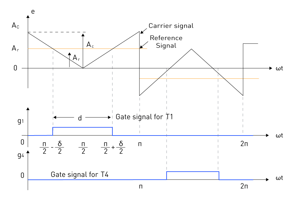
Figure 24: Single Pulse Width Modulation Gating Signals Generation
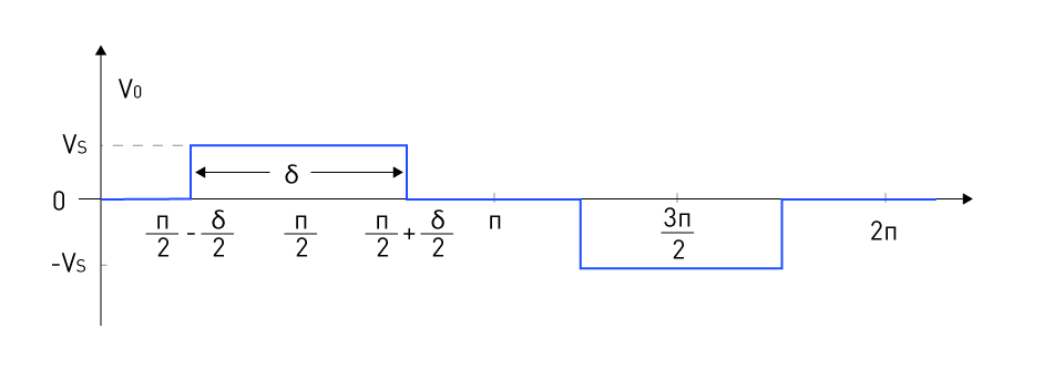
Figure 25: Single Pulse Width Modulation Output Waveform
Figure 24 illustrates the single-pulse width modulation; a straightforward PWM approach that includes creating gating pulses with adjustable width and position. When the modulation index M, which is the ratio of the reference signal Ar to the maximum value of the carrier signal Ac, varies, the position and breadth of this pulse inside each half-cycle also changes, or modulates.
Figure 25 depicts a single-phase full-bridge inverter. A carrier signal is compared to a reference signal to produce gating pulses for switches T1 (and T2), referred to as g1, and T3 (and T4), referred to as g4 as indicated in Figure 24. The positive magnitude of reference and carrier signal determine g1, while g4 is determined by their negative magnitudes. Figure 25 displays the output voltage as a result.
The third harmonic is prominent in this PWM. The distortion factor (DF) is defined as the ratio of the root mean square of harmonics to the fundamental component, with second-order attenuation (division by the square of each harmonic order). It takes into consideration the fact that the output filter would more effectively attenuate harmonics. DF grows as M decreases, implying lower output voltages. Finally, an acceptable value of M is approximately 0.8, where the DF is the smallest.
Multiple-Pulse Width Modulation
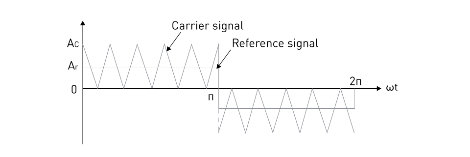
Figure 26: Gate Signal Generation in Multiple-Pulse Width Modulation
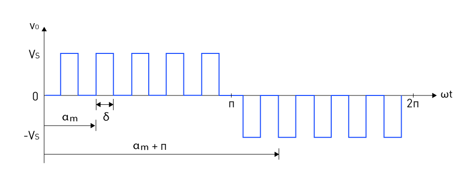
Figure 27: Output Voltage in Multiple-Pulse Width Modulation
A train of pulses can be produced in each half-cycle of the output voltage to lower the output harmonic content. As illustrated in Figure 26, several gating pulses can be created by comparing a reference signal to a triangle carrier signal. As with single pulse width modulation, g1 is determined by a single sinusoidal comparison, and g4 is determined by a comparison with 180° out of phase. The number of pulses in each half-cycle is determined by the carrier frequency. Furthermore, the frequency of the reference signal influences the frequency of the output signal. Finally, the modulation index regulates the output RMS voltage. Figure 27 depicts the resultant output voltage waveform.
When compared to single-pulse width modulation, the DF for multiple-pulse width modulation is substantially lower. However, switching losses rise as the number of switching cycles increases.
Sinusoidal Pulse Width Modulation (SPWM)
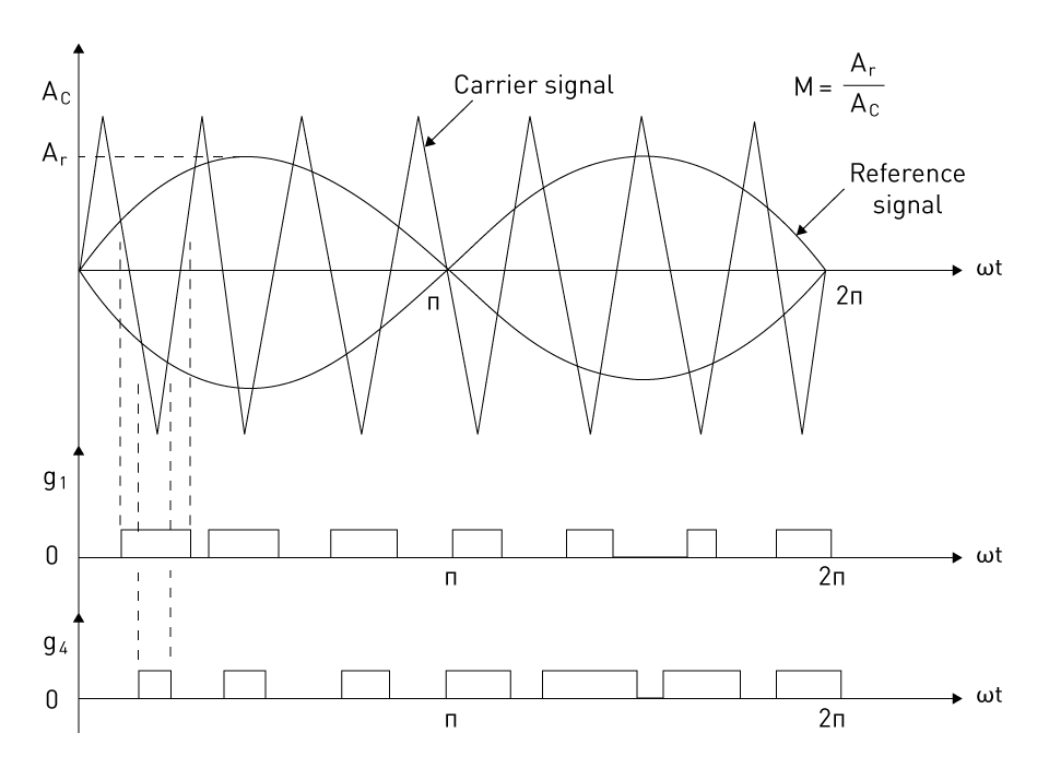
Figure 28: Gate Signal Generation in Sinusoidal Pulse Width Modulation
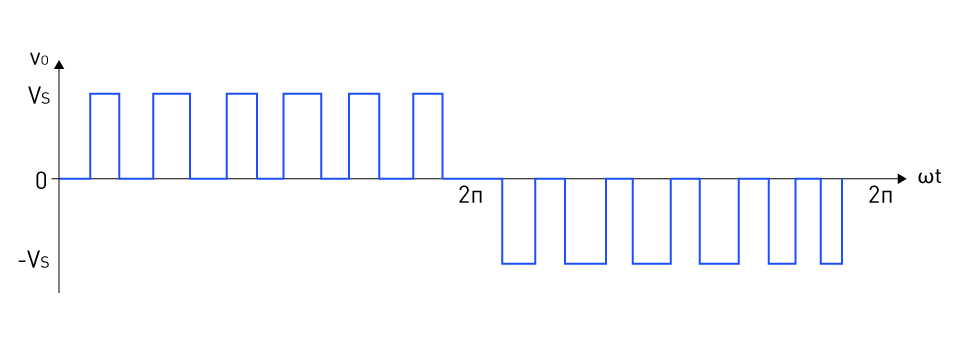
Figure 29: Output Voltage Waveform in Sinusoidal Pulse Width Modulation
Sinusoidal Pulse Width Modulation (abbreviated as SPWM) is a more complex type of PWM. In Figure 29, SPWM generates a pulse train for each gating signal g1 and g4 by comparing a sinusoidal reference signal with a triangular carrier signal. Each pulse's width fluctuates in proportion to the amplitude of a reference sine wave at its center. The reference signal frequency determines the output signal frequency in SPWM. Furthermore, the peak amplitude of the reference signal influences the modulation index M, which controls the output RMS voltage. The number of pulses in each output signal cycle is determined by the carrier frequency. It is worth mentioning that no two switches in the same bridge arm conduct at the same time. Figure 29 depicts a typical output voltage waveform in SPWM. When compared to single and multiple-pulse width modulation methods, SPWM delivers greater harmonic rejection capabilities with much lower order harmonics and DF.
Other SPWM variations exist, such as where the carrier signal is only applied during the first and last 60-degree intervals of half cycles, which improves the output harmonic qualities.
Selective Harmonic Elimination (SHE)
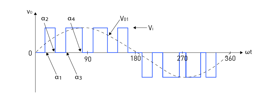
Figure 30: Typical Output Waveform for 3rd, 5th, and 7th Harmonic Elimination with SHE Modulation
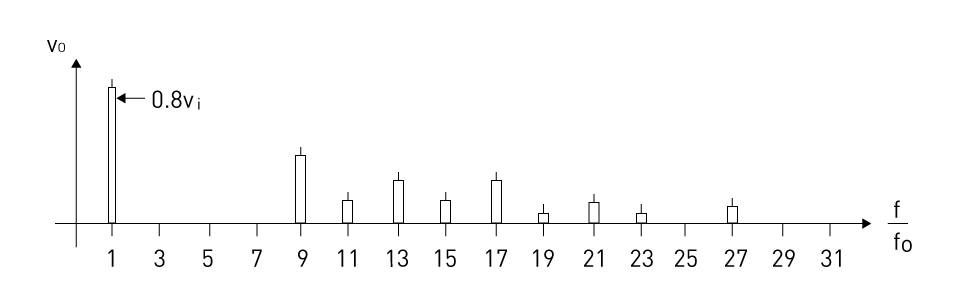
Figure 31: Gate Signal Generation in SHE Modulation
Selective Harmonic Elimination (SHE) is a PWM method for removing certain harmonics from the output waveform. Even harmonics are naturally present in the output; as a result, SHE seeks to reduce the odd harmonics in the single-phase inverter output. SHE entails calculating a series of nonlinear equations using sinusoids in order to obtain the ideal gate switching angles, such as α1, α2, α3, αN. In general, N half-cycle pulses (switching angles) are necessary to alter the fundamental component and eliminate N-1 harmonics. N nonlinear equations are solved to find the switching angles. Figure 30 depicts a typical output waveform with the removal of 3rd, 5th, and 7th harmonics. Figure 31 depicts the frequency spectrum corresponding to the produced output signal in Figure 30.
Three-Phase Inverters
Three-phase inverters can be thought of as three single-phase inverters, with the output of each single-phase inverter shifted by 120-degree. Thus, the PWM methodologies discussed above for single-phase inverters are still applicable. In SPWM, for example, three sinusoidal references produced 120-degree apart are compared with the carrier signal to provide the appropriate gating signals for the phase.
There are various innovative ways for three-phase inverters that leverage their unique structure.
Third-Harmonic PWM
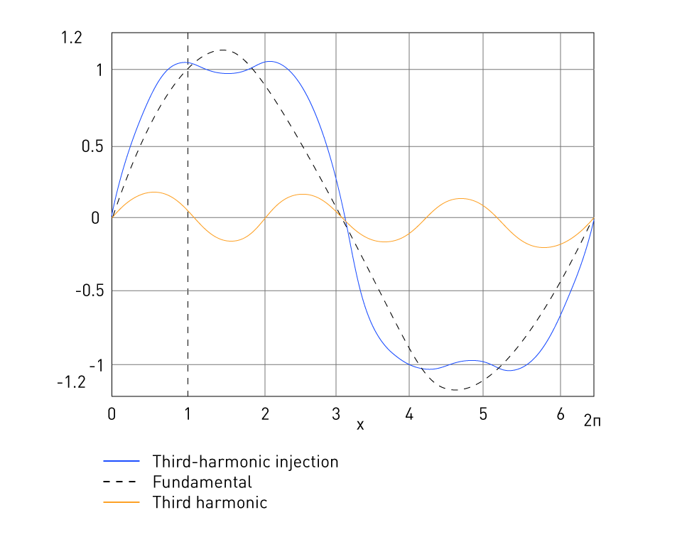
Figure 32: Reference Signal Generation in Third-Harmonic PWM
The reference signal in the third-harmonic PWM for three-phase inverters is made up of the fundamental signal as well as its third harmonic, as shown in Figure 32. The third harmonic component in the neutral terminal is effectively canceled when a third harmonic component is present in each phase. By offering a fundamental component that is around 15.5% greater than that of sinusoidal PWM, third-harmonic PWM offers superior dc supply voltage consumption than sinusoidal PWM.
Space-Vector Modulation
SVM is an advanced pulse width modulation (PWM) technology that is typically employed in three-phase inverter systems. It has advantages such as higher source usage and lower harmonics when compared to other approaches such as 180-degree conduction, SPWM, and so on. SVM is a digital modulating technique that generates PWM load line voltages that are on average equal to a given (or reference) load line value. SVM has received significant popularity in a variety of applications, including motor drives, renewable energy systems, and uninterruptible power supplies, because of its ability to maximize inverter performance.
The fundamental distinction between SVM and traditional PWM approaches is in the mathematical formulation and production of switching patterns. The output voltage is represented as a vector in a complex plane known as the α-β plane by SVM, and the proper switching states are determined to yield the required voltage vector.
Principles of Space Vector Modulation
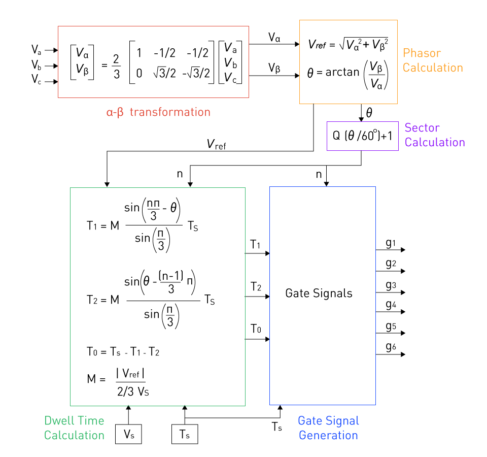
Figure 33: Block Diagram of the SVM Technique
Figure 33 shows the block diagram of the SVM technique for gate signal generation. The key functional components in the SV M method are discussed as follows.
α-β transformation: Using the α-β transformation, the reference three-phase voltages are first represented in a two-dimensional plane. The three-phase voltage space vectors Va, Vb, and Vc are projected onto the α-β plane, yielding a single vector with two components, Vα and Vβ. The formulae for the transformation are illustrated in the alpha-beta transformation block as depicted in figure 33.
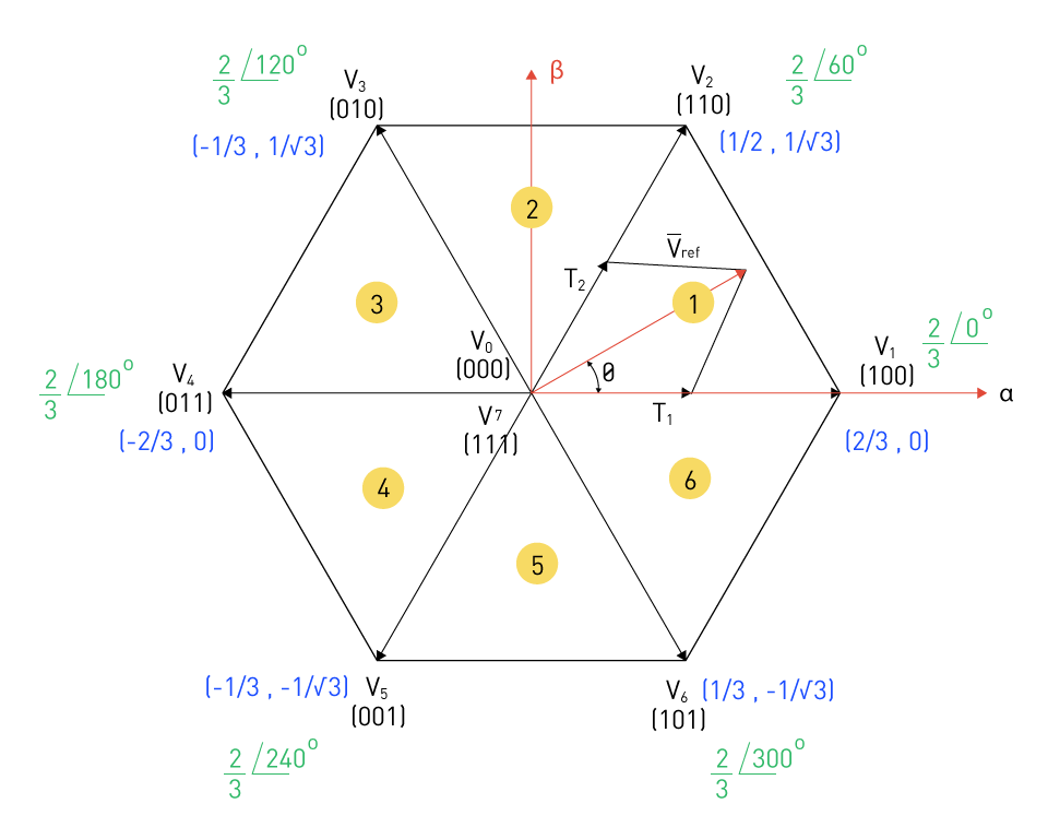
Phasor Calculation: Following that, the Vα and Vβ components are transformed into phasors to estimate their magnitude Vref and angle θ on the α-β plane using the equations in Figure 33's phasor calculation block. Figure 34: The Inverter Switching States Figure 35: Calculation of Sector and Adjacent Switching States Sector Calculation: Table 1 depicts a three-phase voltage source inverter (VSI) with eight different switching states controlled by the on/off position of the six power switches. There are six active states and two null states. Figure 34 depicts the inverter configurations associated with the valid states. As illustrated in Figure 35, the space vectors associated with the valid states are positioned on a hexagon in the - plane, whereas the zero vectors are located at the origin. The active sector in which the reference vector is located is found using n=Q( θ/60°)+1, where Q is the fraction's quotient. Table 1: Valid Switching States and Associated Normalized Space Vectors in 3-Phase VSIs Dwell time calculation: SVM's goal is to generate the required output voltage by selecting appropriate space vectors that correspond to the valid states and their dwell durations (the length for which each vector is applied). By correctly choosing and employing these vectors at a particular switching period, the required output voltage may be synthesized (on average). The dwell periods are determined in such a way that the average voltage vector for a switching period is close to the intended output voltage vector. Figure 33's dwell time block depicts the equations needed to calculate dwell time for each condition. This block's inputs are the source voltage Vs and the switching time Ts. Using Vs and Vref, the modulation index M can be calculated, which can then be used to calculate the timings T1 and T2 in each of the neighboring valid states, as well as the time T0 in the null state. Because the times can only be positive, the value of M varies from 0 to √3/2. Note: Overmodulation (also known as six-step operation) is another option for operating the inverter; however, this might result in increased output distortion.
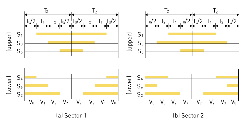
Table 2: Switching Pattern for all SVM Sectors Gate Signal Generation: The gate signal is generated in the final phase of SVM. The gate signal generation block receives information about the dwell periods for each switching state for each sector. The switching pattern for each SVM sector is displayed in Table 2. In order to reduce even harmonics, these patterns are constructed to ensure that the output voltages have quarter-wave even symmetry. In order to reduce switching losses, it also made sure that only one bit at a time in the switching pattern is modified. Similar to this, the zero-vectors corresponding to the null states are chosen such that the switching pattern is altered as little as possible when moving between these states. Figure 36: Switching patterns and the dwell times for Sector 1 and 2 Figure 36 reflects the Sectors 1 and 2's switching patterns and accompanying dwell periods. Similar patterns can be seen for other industries as well. Switches Q1-6 in the 3-phase bridge inverter can be triggered utilizing the gating sequence. Figure 37: Example output voltage in SVM The typical example of the inverter line output voltage utilizing SVM modulation is shown in Figure 37 together with the basic component. Although they resemble Voltage Source Inverters (VSIs), Current Source Inverters (CSIs) are a beneficial class of DC/AC converters that have their own characteristics setting them apart from VSIs. The use of a current source as opposed to a voltage source makes CSIs stand out as a group. This implies that regardless of the load, the current output is constant. This stands in stark contrast to VSIs, which emit a constant voltage. As a result, CSIs are particularly well suited for applications that demand consistent current because their output current is insensitive to variations in the load or line impedance. Since the attributes of one can be changed into the other by switching the roles of voltage and current and substituting impedance with its reciprocal, CSIs and VSIs can be thought of as duals of one another. For instance, VSIs use big capacitors to keep the voltage constant, while CSIs use big inductors to keep the current constant. This duality also applies to their control strategies and safeguards, with VSIs requiring overcurrent safety while CSIs need overvoltage safety. Though CSIs have benefits like built-in short-circuit protection and higher performance with inductive loads, it's important to remember that they can be more difficult to design and manage, and they might not be appropriate for many applications. During the inverter design process, a few significant general design issues must be addressed. The loading requirements determine the inverter's fundamental design. The selected inverter topology, load, and control methods determine the voltage and current ratings of power devices in inverters. It is necessary for the design to (1) assess the instantaneous load current and (2) plot or simulate the current flowing through each component. Once the current levels are understood, it is possible to determine the ratings of power devices. The reverse voltages of each device must be identified in order to assess the voltage ratings of the devices. These can be calculated analytically or numerically and verified by simulation. Last but not least, correctly designed output filters are required to assure power quality and harmonics reduction. There are numerous fundamental types of filters available, including C-filter, LC-tuned filter, CLC-filter with their respective merits/demerits. Efficiency and power quality are key concepts for inverters, just like they are for other power converters. An inverter's efficiency depicts how well input DC power is converted into output AC power. Switching, heat, and standby power all result in a loss of power. An inverter's efficiency is where PAC is AC power output and PDC is DC power input. High-quality sine wave inverters often have peak efficiencies ranging from 90 to 95%. Modified sine wave inverters of lower quality are 75–85% efficient. High frequency inverters typically outperform their low frequency equivalents in terms of efficiency. The efficiency of the inverter is determined by the load. With a few minor deviations, the efficiency is almost at its highest at high output power. Nevertheless, the efficiency is quite low when power output is less than 10-15%. This can be explained by the fact that an inverter's stand-by losses are constant across all output power levels, reducing efficiency at lower outputs. Power quality is an analogous concept of the inverter output. Generally, the output power should be sinusoidal with little harmonic content. Harmonics may lead to unwanted consequences including decreased power efficiency, unnecessary overheating, shortened equipment life, etc. Therefore, to reduce harmonics, PWM methodologies and filters are required.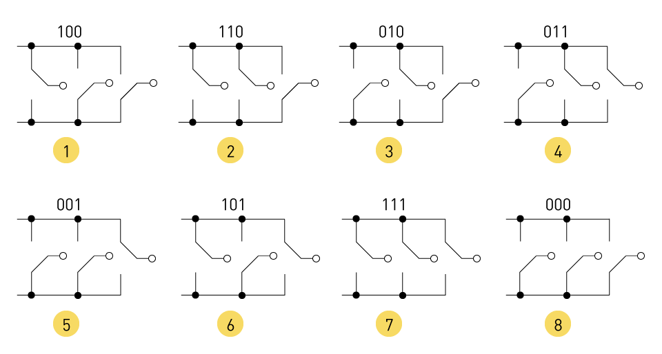
Voltage Vectors
Switch States
Line to Neutral Voltages
Space Vectors
V1
a
b
c
Van
Vbc
Vcn
1
0
0
$$\frac{2}{3}$$
$$\frac{-1}{3}$$
$$\frac{-1}{3}$$
$$(\vec{Q}=\frac{2}{3}+0j=\frac{2}{3}0°)$$
V2
1
1
0
$$\frac{1}{3}$$
$$\frac{1}{3}$$
$$\frac{-2}{3}$$
$$(\vec{Q}= \frac{1}{3}+ \frac{1}{\sqrt{3}}j=\frac{2}{3}60°)$$
V3
0
1
0
$$\frac{-1}{3}$$
$$\frac{2}{3}$$
$$\frac{-1}{3}$$
$$(\vec{Q}= \frac{-1}{3}+ \frac{1}{\sqrt{3}}j=\frac{2}{3}120°)$$
V4
0
1
1
$$\frac{-2}{3}$$
$$\frac{1}{3}$$
$$\frac{1}{3}$$
$$(\vec{Q}= \frac{2}{3}+ 0j=\frac{2}{3}180°)$$
V5
0
0
1
$$\frac{-1}{3}$$
$$\frac{-1}{3}$$
$$\frac{2}{3}$$
$$(\vec{Q}= \frac{-1}{3}+ \frac{1}{\sqrt{3}}j=\frac{2}{3}240°)$$
V6
1
0
1
$$\frac{1}{3}$$
$$\frac{-2}{3}$$
$$\frac{1}{3}$$
$$(\vec{Q}= \frac{1}{3}+ \frac{1}{\sqrt{3}}j=\frac{2}{3}300°)$$
V0
0
0
0
0
0
0
$$(\vec{Q}= 0+ 0j=0 0°)$$
V7
1
1
1
0
0
0
$$(\vec{Q}= 0+ 0j=0 0°)$$
Sector
Segment
1
2
3
4
5
6
7
1
Vector State
V0
000V1
100V2
110V7
111V2
110V1
100V0
000
2
Vector State
V0
000V3
010V2
110V7
111V2
110V3
010V0
000
3
Vector State
V0
000V3
010V4
011V7
111V4
011V3
010V0
000
4
Vector State
V0
000V5
001V4
011V7
111V4
011V5
001V0
000
5
Vector State
V0
000V5
001V6
101V7
111V6
101V5
001V0
000
6
Vector State
V0
000V1
100V6
101V7
111V6
101V1
100V0
000

Current Source Inverters (CSIs) - Duals of Voltage Source Inverters (VSIs)
Design Considerations
Efficiency and Power Quality In Inverters
Log in to your account
Create New Account